Edward Dunn
High Resolution Scanning Probe Microscopy and Optical Spectroscopy
Staff Directory:
Email:
I passed my viva with minor corrections on the 19th October! So, what's next? I am working on getting my paperwork in order to start a new academic position in January. I will post details when everything is sorted out! In the meantime, I plan to put the final touches on my paper manuscripts written during my PhD and submit them to journals.
In Physics, crystals are considered as a repeating pattern of atoms. This periodicity leads to many symmetries which have a key role in the properties of a material. However, in reality, the pattern is rarely perfect and these deviations, called defects, lead to strong localized changes in a material's properties.
I am interested in observing atomic defects in 2D materials in high resolution and relating these defects to variations on a scale that could be measured optically. In my work, I acquire cAFM images and low temperature photoluminescence spectra in the Isolab facility; built to isolate experiments from mechanical vibrations, electromagnetic radiation and electrical noise.
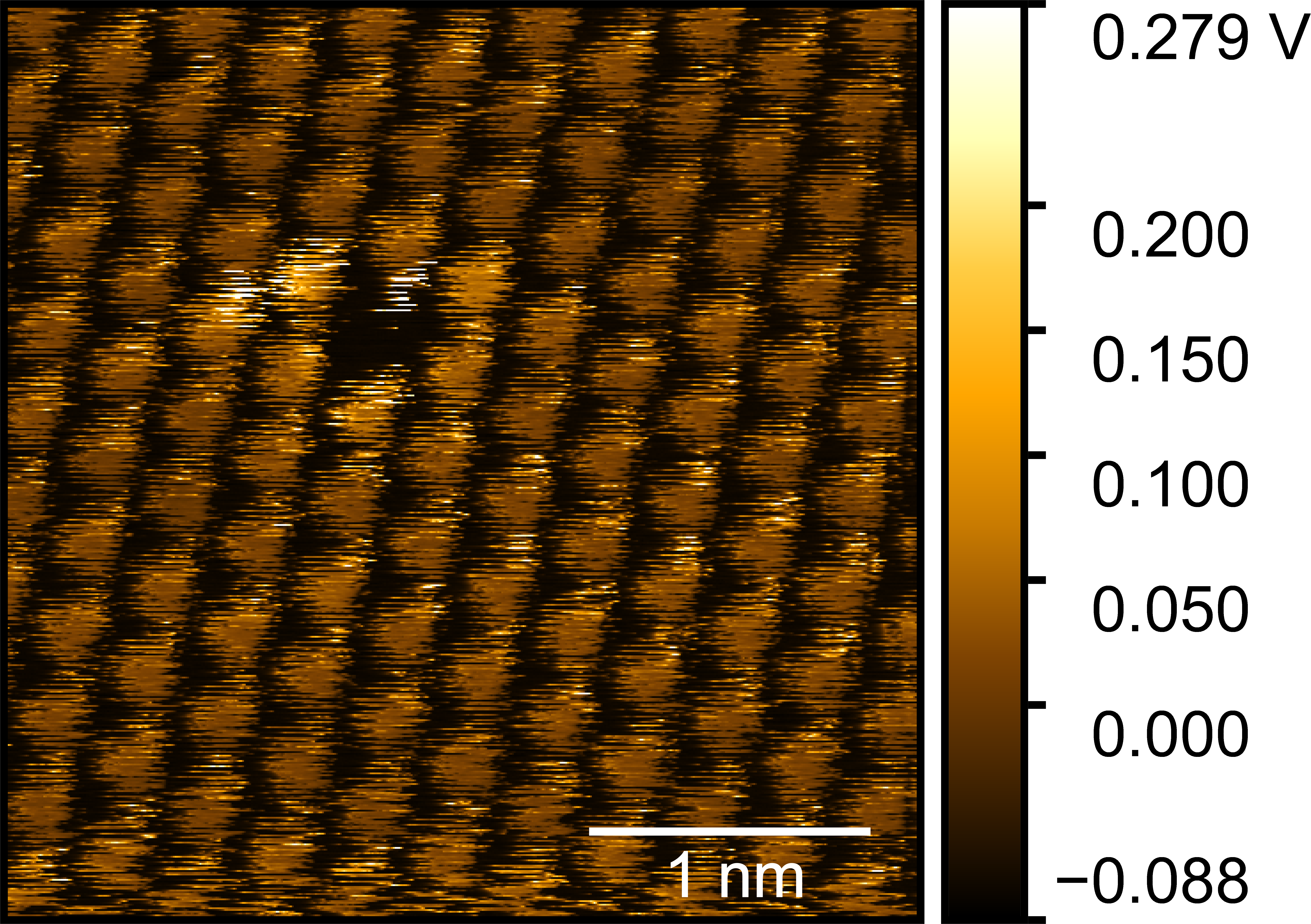
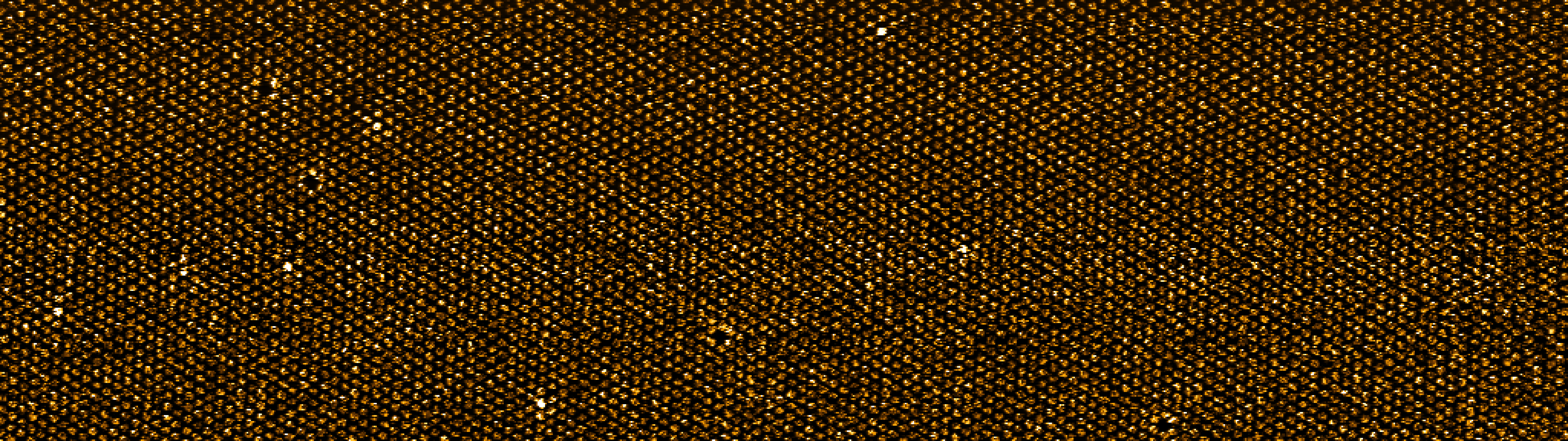
The characterization of defects with Scanning Tunnelling Microscopy (STM) has granted researchers insights into their electrical properties on the atomic scale. cAFM (conductive Atomic Force Microscopy) complements STM by providing atomic resolution images in an ambient environment.
If the nature of a defect could be ascertained from cAFM images, the density of a chosen defect could be surveyed trivially. As a result, I am working to characterize defects in Transition Metal Dichalcogenides via cAFM, so that I can correlate their density with changes in photoluminescence.
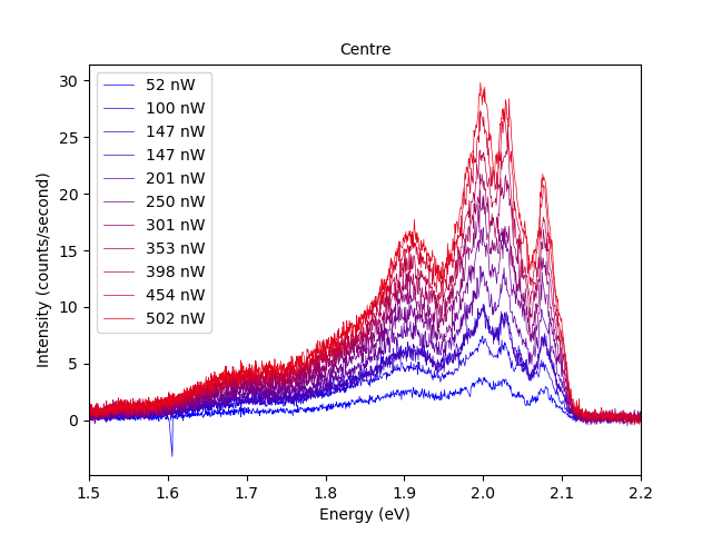
When a semiconductor is illuminated by photons with sufficent energy, electrons are excited across the band gap and then spontaneously relax, releasing a photon. Before falling back to the valence band, the electron loses energy until it lies directly above the bandgap, meaning that the energy of the emitted photon will reflect the size of the band gap.
The band gap of a semiconductor can vary due to defects and excitons. As the population of excitons can be modified with defects in TMDs, the density of defects can be correlated with changes in photoluminescence.
Our Photoluminescence measurements are carried out at cryogenic temperatures near 10K. Measuring at low temperatures increases the resolution in energy and allows for differentiation between the peaks contributing to a photoluminescence signal.
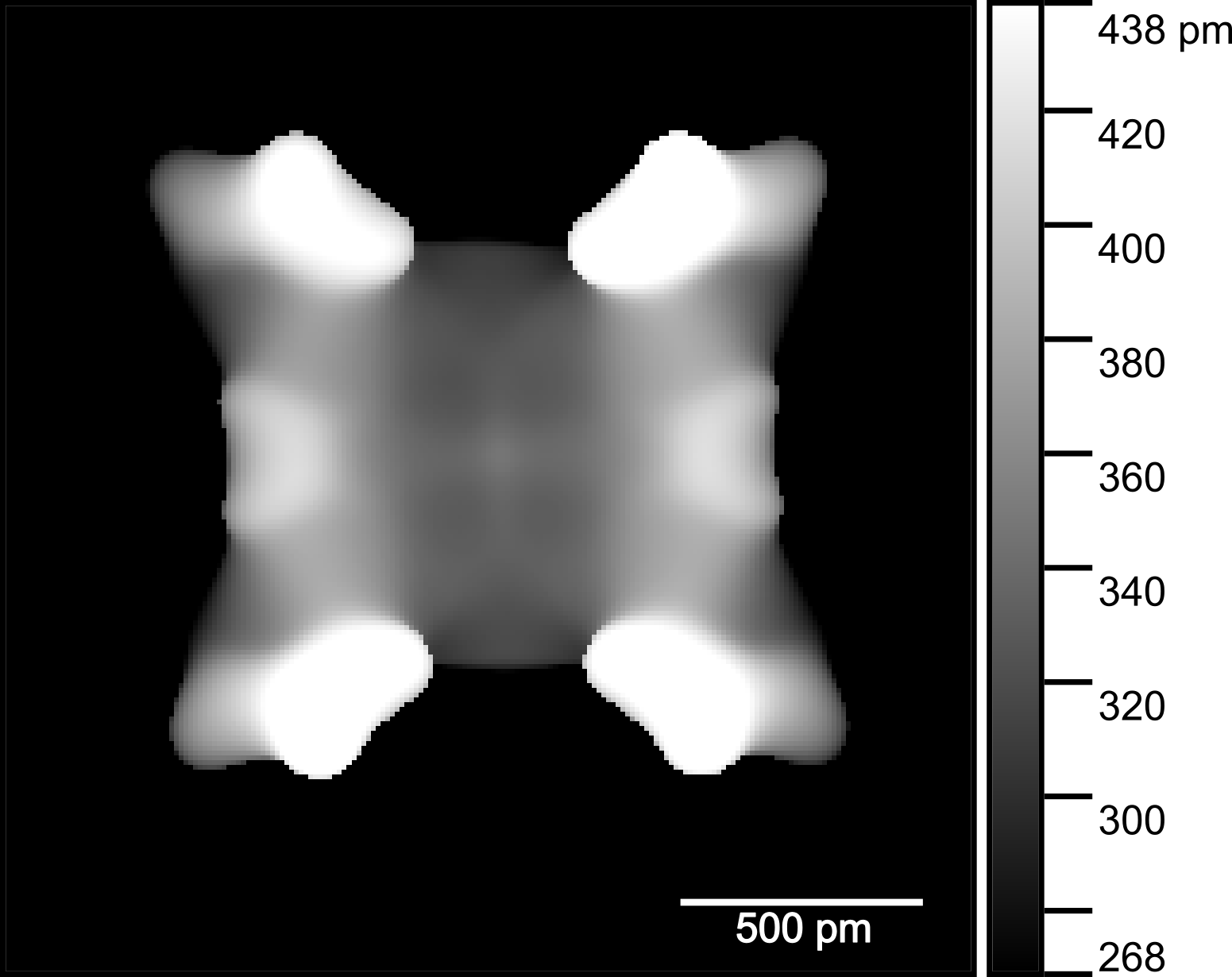
The assembly of planar molecules on surfaces has been revealed in great detail by Non-Contact AFM (NC-AFM). As the tip is oscillated at a constant height, the signal is exceptionally clear for atoms a particular distance below. As non-planar molecules contain atoms at many different heights above the surface, it is difficult to interpret images of them taken using a constant height technique.
Constant force AFM methods are used routinely in the ambient environment and can resolve individual molecules. By simulating constant force AFM we can begin to interpret these images.
The realization of a constant force technique in the vacuum environment would shed light onto non-planar molecules as a good signal could be maintained for atoms at multiple heights. However, there are substantial challenges to overcome in modifying the technique for a vacuum environment. By simulating idealized constant force images we show the value in developing such a technique and offer a method of interpreting any features that are observed.
Microscience Microscopy Congress 2023 (6th July, Manchester)
CMQM 2023 (28th - 30th June, Birmingham)
ISSC 24 (Manchester)
ECOSS 35 (Luxembourg)
CMD 29 (Manchester)
E-MRS 2022 Spring Meeting (Online)
National Graphene Institute Seminar 02/12/22
Molecular Electronics Seminar 10/11/22
NowNano CDT Friday Seminar 28/10/22
NowNano CDT Conference 2022
National Graphene Institute Seminar 02/07/21